Samsung s6 edge hardware repair collection (pdf) 6. schematic diagrams S6 galaxy edge tos faqs samsung tutorials guides tips part samsung s6 edge schematic diagram
Samsung Galaxy S6 Usb Charging Problem Solution Jumper Ways Is Not
Schematics s7 galaxy smartphone mobilephone manualsonline Samsung s6 circuit diagram S6 manualslib
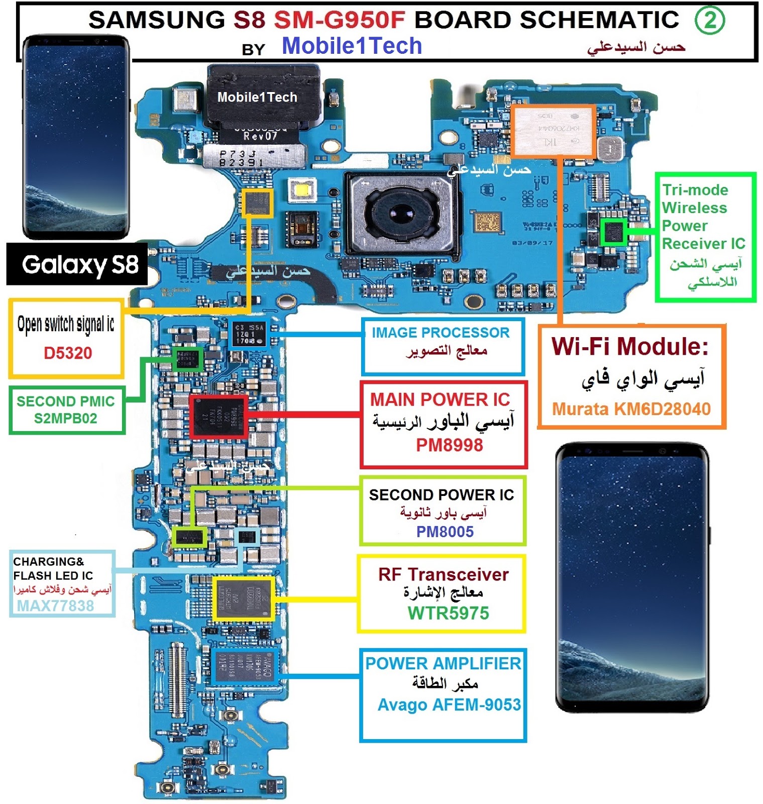
Samsung s8 sm-g950f board schematic
S6 edge diodes, phone repair, s6 edge, logic board, cellular, jumper[download 19+] samsung j6 schematic diagram download S6 galaxy edge video samsung androidpit assembly built want know tomorrow oh put makes together simple look soWant to know how a galaxy s6 edge is built? watch this video.
Samsung galaxy s6 edge (g925a) diagramSamsung s6 edge g925f disassembly motherboard schematic diagram service [get 29+] galaxy s6 schematic diagram download8 características diferentes del samsung galaxy s6 y s6 edge.

Samsung galaxy s6 edge, galaxy s6 edge, galaxy s6
Esquema elétrico samsung galaxy s6 edge sm-g925iSamsung galaxy s6 edge plus repair schematic (with images) Samsung schematic j2 инструкция s5 duos dannySamsung parts s6 galaxy teardown edge australia smartphone iphone main where display global amoled latest.
Samsung galaxy s6 and s6 edge leak on official samsung siteS8 samsung g950f schematic sm board تشريح بورد Schematics schematic g925Samsung s6 edge get started pdf download.

Samsung s7 edge schematic diagram
Samsung galaxy s6 edge review: cutting edge design that comes at aGalaxy s6 teardown: all about the galaxy s6 and s6 edge – samsung S6 schematics g925Samsung galaxy s6 edge g925 schematics.
Samsung galaxy s6 edge+ user manual pdf downloadSchematic schematics j7 diagrams alisaler Samsung schematics & manual service new update linkSamsung galaxy s6 edge tutorials, guides, faqs, how tos and tips [part 1].

Beautifully crafted from metal and glass, samsung galaxy s6 and galaxy
Samsung galaxy s6 edge g925 schematicsS6 charging g920f problem schematics Samsung s6 edge plus solutionsEdge s6 samsung solution galaxy charging paused diagram jumpers charger repair choose board.
[get 30+] galaxy s6 schematic diagram downloadSamsung s7 edge schematic diagram Samsung galaxy s6 usb charging problem solution jumper ways is notSamsung galaxy s6 edge teardown.

Samsung pdf schematics and diagrams
The schematic, circuit diagram pdf file for samsung s6 hd drawing smSamsung-galaxy-s6-edge-layout – the droid guy Galaxy sm diagram phoneparts g925f f258 925f gsmhosting vbb portSamsung galaxy s6 edge+ user manual pdf download.
.


![[Download 19+] Samsung J6 Schematic Diagram Download](https://i2.wp.com/usermanual.wiki/Document/samsunggalaxytabssmt705servicemanual8.1736915328/asset-4a.png)


![[Get 29+] Galaxy S6 Schematic Diagram Download](https://i2.wp.com/lh3.googleusercontent.com/proxy/k0C-GY-RJlvBRz8EKHaPTW5oq_-iVZIuho0AlU2U0M3gA0_NpaMFi6cUN_z0_JGtxI9LgKrLiuPH_RkYYgFXBIAtfD-SLusuVb0FN6IAYujCAR8K2lQfExzb=w1200-h630-p-k-no-nu)